


リンクフリーです。
バナーをお使いください。
|

|
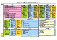
※上記からプログラムのダウンロードが可能です。 |
3/6 (日)
| 17:30- |
受付 |
| 18:00-19:30 |
ウェルカムパーティ (名古屋工業大学 カフェサラ) |
3/7 (月)
| 8:45- |
受付 |
開会/特別講演
座長: 増田秀樹 (名古屋工業大学)
A会場 |
| 9:15-9:30 |
開会挨拶
【来賓挨拶】
常盤豊(文部科学省 高等教育局 主任視学官(科学技術・学術総括官))
【主催者挨拶】
松尾稔((財)科学技術交流財団 理事長)
【ISPlasma2011組織委員会委員長挨拶】
堀勝(名古屋大学) |
| 9:30-9:40 |
開会の辞
大塚美則((財)科学技術交流財団 東海広域知的クラスター創成事業本部 事業総括)
"Tokai Region Nanotechnology Manufacturing Cluster and its Expansion Program" |
| 9:40-10:10 |
特別講演 7a-A01PL
榊裕之(豊田工業大学)
"From Superlattices to Quantum Dots: Roles of Nanostructures in Advanced Electronics and Photonics" |
| 10:10-10:30 |
休憩 |
基幹講演/東海広域クラスター講演
座長: 野田正治((財)科学技術交流財団)
A会場 |
| 10:30-11:00 |
基幹講演 7a-A02SK
John Robertson (Cambridge University, UK)
"Applications of Carbon Nanotubes Grown by Chemical Vapor Deposition" |
| 11:00-11:20 |
東海広域ナノテクものづくりクラスター講演 7a-A03C
堀勝(名古屋大学)
"Fundamental Research and Global Innovation on Plasma Nanoprocessing" |
| 11:20-11:35 |
東海広域ナノテクものづくりクラスター講演 7a-A04C
江川孝志(名古屋工業大学)
"Study on AIGaN/GaN HEMT Grown on Si Substrate" |
| 11:35-11:50 |
東海広域ナノテクものづくりクラスター講演 7a-A05C
高井治(名古屋大学)
"Material Development by Means of Solution Plasma" |
| 11:50-12:05 |
東海広域ナノテクものづくりクラスター講演 7a-A06C
渡辺義見(名古屋工業大学)
"Drilling of Carbon Fiber Reinforced Plastic by Gyro-driven Metal-bonded Grinding Wheel" |
| 12:05-13:00 |
昼食 |
| 13:00-14:30 |
ポスターセッション 1 |
| |
プラズマ科学1
先進プラズマ計測技術
座長: D. Graves (University of California, Berkeley, USA)
A会場 |
窒化物半導体1
プラズマ支援成長
座長: N. Grandjean
(EPFL, Switzerland)
B会場 |
ナノ材料1
ナノパーティクル
座長: 日原岳彦
(名古屋工業大学)
C会場 |
14:30-15:00
基調講演
7p-A01KA
U. Czarnetzki (Ruhr-Univ, Bochum, Germany)
"Determination of Electron Densities by Diode Laser Absorption Spectroscopy" |
14:30-15:00
基調講演
7p-B01KB
B. Daudin (CEA Grenoble, France)
"Growth, Structural and Optical Properties of InGaN/GaN Nanowires" |
14:30-15:00
基調講演
7p-C01KC
小田正明((株)アルバック)
"Individually Dispersed Nanoparticles by Gas Evaporation and their Applications" |
15:00-15:30
基調講演
7p-A02KA
J. P. Booth (CNRS, France)
"Seeing Inside Plasma Etch Reactors: From Diagnostics to Sensors for Control" |
15:00-15:20
7p-B02OB
Y. Kawai (Nagoya University, Japan)
"Realization of Excellent Crystalline Quality of AlGaN Epilayer Grown on AlN Template by Plasma-Assisted Molecular Beam Epitaxy" |
15:00-15:20
7p-C02OC
R. Boswell (Australian National University, Australia)
"Low Temperature Sputtering of Nanocrystalline N-doped TiO2 Thin Films with Ar/O2/N2 Helicon Plasma" |
15:30-15:50
7p-A03OA
I. Liang (Chubu University, Japan)
"Electron Density Measurement by Novel Frequency Shift Probe" |
15:20-15:40
7p-B03OB
T. Ohachi (Doshisha University, Japan)
"Parallel Mesh Electrode to Monitor Nitrogen Atoms for Growth of III Nitride Semiconductors by PA-MBE" |
15:20-15:40
7p-C03OC
S. Yooyen (Mie University, Japan)
"Pulse Plasma CVD on the Growth of Nanorod" |
15:50-16:10
7p-A04OA
N. Sumi (Nagoya University, Japan)
"Real-time Electron-spin-resonance Measuremnt of Plasma Induced Surface Interactions" |
15:40-16:00
7p-B04OB
J. Birch (Linkoping University, Sweden)
"Ion-assisted Magnetron Sputter Epitaxy of Group III-nitrides" |
15:40-16:00
7p-C04OC
S. Machmudah (Kumamoto University, Japan)
"Gold and Silver Nanopaticles Produced by Pulsed Laser Ablation in Supercritical CO2" |
16:10-16:20
休憩 |
16:00-16:20
休憩 |
16:00-16:20
休憩 |
プラズマ科学2
シミュレーション
座長: U. Czarnetzki
(Ruhr-University Bochum, Germany)
A会場 |
窒化物半導体2
光デバイス
座長: F. Ponce (Arizona State University, USA)
B会場 |
ナノ材料2
表面改質・表面機能化
座長: 牧原克典
(名古屋大学)
C会場 |
16:20-16:50
基調講演
7p-A05KA
D. Graves (University of California, Berkeley, USA)
"Plasma-Surface Interactions at the Nanometer Scale" |
16:20-16:50
基調講演
7p-B05KB
N. Grandjean (EPFL, Switzerland)
"AlInN Alloy for Electronic and Optoelectronic Applications" |
16:20-16:50
基調講演
7p-C05KC
滝川浩史(豊橋技術科学大学)
"Super Hard Diamond-like Carbon Films; A State-of-the-Art" |
16:50-17:10
招待講演
7p-A06IA
S-Y. Kang
(Tokyo Electron Ltd. Technology Development Center, Japan)
"The Effect of Additional Database on Plasma Simulation for Etching Process" |
16:50-17:10
7p-B06OB
W. Y. Weng (National Cheng Kung University, Taiwan)
"High Responsivity GaN Nanowire-based UV Photodetectors" |
16:50-17:10
7p-C06OC
J-H. Jin (Korea University, Korea)
"Effects of Plasma Surface Functionalization on Biosensing Characteristics of A Fully-Integrated CNT-based Electrode System on Glass Substrate" |
17:10-17:30
招待講演
7p-A07IA
Y. Tanaka (Kanazawa University, Japan) "Numerical Thermofluid Model of High-Power High-Pressure ICPs with Molecular Gases using Reaction Kinetics" |
17:10-17:30
7p-B07OB
H. S. Jeon (Korea Maritime University, Korea)
"UV LED with High Quality Epilayer grown by HVPE" |
17:10-17:30
7p-C07OC
C. Geffers (RWTH Aachen University, Germamy)
"Nanophase Hardfaced Coatings" |
| 17:30-19:00 |
ポスターセッション 2 |
3/8 (火)
| 9:00- |
受付 |
| |
プラズマ科学3
エッチングプロセスⅠ
座長: F. Laermer (Robert Bosch GmbH, Germany)
A会場 |
窒化物半導体3
デバイス評価
座長: 徳田豊
(愛知工業大学)
B会場 |
ナノ材料3
リチウム電池
座長: 川崎晋司
(名古屋工業大学)
C会場 |
9:20-9:50
基調講演
8a-A01KA
M. J. Goeckner (University of Texas, Dallas, USA)
"An Improved Understanding of Fluorocarbon Plasmas" |
9:20-9:50
基調講演
8a-B01KB
F. Ponce (Arizona State University, USA) "Polarization Effects in Group-III Nitride Semiconductor Heterostructure Devices" |
9:20-9:50
基調講演
8a-C01KC
吉野彰(旭化成(株))
"Latest trends of Lithium Ion Battery Technology and Market" |
9:50-10:20
基調講演
8a-A02KA
A. Wendt (University of Wisconsin - Madison, USA)
"Control of Bombarding Ion Energy Distributions in Plasma Processing" |
9:50-10:10
8a-B02OB
Z. Chen (Nagoya Institute of Technology, Japan)
"Optical Properties and Deep Traps of InAlN Lattice-Matched to GaN Grown by MOCVD" |
9:50-10:10
8a-C02OC
N. Imanishi (Mie University, Japan)
"High Performance Si/Disordered Carbon with CNFs Composites for Lithium Ion Batteries" |
10:20-10:40
8a-A03OA
K. Hirota (Hitachi, Ltd., Japan)
"Study of Process Drift Caused by Ti Residue on Reactor Walls in Metal Gate Ethcing" |
10:10-10:30
8a-B03OB
Y. Nakano (Chubu University, Japan)
"Correlation between Current Collapses and Deep-Level Defects in AlGaN/GaN Hetero-Structures Probed by Photo-Capacitance Spectroscopy" |
10:10-10:30
8a-C03OC
Z. Quan (Nagoya Institute of Technology, Japan)
"Electrochemical property of LiCoO2 thin films composed of nanoparticles" |
10:40-10:50
休憩 |
10:30-10:50
休憩 |
10:30-10:50
休憩 |
プラズマ科学4
エッチングプロセスⅡ
座長: M. J. Goeckner (University of Texas, Dallas, USA)
A会場 |
窒化物半導体4
GaN/Siとその応用
座長: 井上薫
(パナソニック(株))
B会場 |
ナノ材料4
ポーラス材料
座長: 猪股智彦
(名古屋工業大学)
C会場 |
10:50-11:20
基調講演
8a-A04KA
F. Laermer (Robert Bosch GmbH, Germany)
"BOSCH-DRIE: Impact on MEMS and Applications" |
10:50-11:20
基調講演
8a-B04KB
A. Krost (Otto von Guericke University Magdeburg, Germany)
"Present and Future of GaN-on-Si" |
10:50-11:20
基調講演
8a-C04KC
H-C. Zhou (Texas A&M University, USA) "Metal-Organic Frameworks for Gas Storage and Separation" |
11:20-11:40
8a-A05OA
J. Ladroue (GREMI-STMicroelectronics, France)
"Deep Gallium Nitride Etching: Ways to Avoid Etching Defects" |
11:20-11:40
招待講演
8a-B05IB
S. Arulkumaran (Nanyang Technological University, Singapore)
"High Off-state Breakdown Characteristics of AlGaN/GaN HEMTs on 4-inch Si" |
11:20-11:40
招待講演
8a-C05IC
S. Furukawa (Kyoto University, Japan)
"An Entangled Porous Framework As a Luminescent Sensor" |
11:40-12:00
8a-A06OA
X. Li (University of Glasgow, Schotland)
"A Low Damage Etchig Process of Sub-100 nm Platinum Gate Line for III-V MOSFET Fabrication and the Optical Emission Spectrometry of the Inductively Coupled Plasma of SF6/C4F8" |
11:40-12:00
8a-B06OB
Y. Liu (Sun Yat-sen University, China)
"Normally-off AlGaN/GaN HFETs on Si (111) Substrate Fabricated by Selective Area Growth Technique" |
11:40-12:00
招待講演
8a-C06IC
A. Takeno (Gifu University, Japan)
"Nano Porous Plymer Film and Fiber by Craze Processing" |
| 12:00-13:00 |
昼食 |
| 13:00-14:30 |
ポスターセッション 3 |
窒化物半導体5 窒化物半導体デバイスの最新の進展
座長: 東脇正高((独)情報通信研究機構 新世代ネットワーク研究センター)
A会場 |
| 14:30-15:00 |
基調講演
8p-A01KB
A. Khan (Unversity of South Carolina, USA)
"Recent Progress of Nitride Semiconductor Devices and the Role of Plasma Science and Technology" |
| 15:00-15:30 |
基調講演
8p-A02KB
D. Alquier (Université de Tours, France)
"Recent Progresses in GaN Power Rectifier" |
| 15:30-16:00 |
基調講演
8p-A03KB
上田大助(パナソニック(株))
"Renovating Power Electronics by III-Nitride Devices" |
| 16:00-16:30 |
基調講演
8p-A04KB
天野浩(名古屋大学)
"Plasma Assisted Molecular Beam Epitaxial Growth of Thick InGaN Films and InGaN Nanorods for Future Light Source" |
| 16:30-16:50 |
休憩 |
窒化物半導体6 プラズマ科学と窒化物半導体Ⅱ
座長:岩崎誠(名古屋工業大学)
A会場 |
| 16:50-18:10 |
パネルディスカッション
先進プラズマ技術の窒化物半導体への応用II
<モデレーター>
名西憓之 (立命館大学, Seoul National University, Korea)
<パネリスト>
D. Alquier (Université de Tours, France)
天野浩(名古屋大学)
B. Daudin (CEA Grenoble, France)
N. Grandjean (EPFL, Switzerland)
加納浩之(NUエコ・エンジニアリング(株))
A. Khan (University. of South Carolina, USA)
E. Monroy (CEA Genoble, France)
徳田豊(愛知工業大学)
上田大助(パナソニック(株))
上殿明良(筑波大学)
|
| 18:30-20:00 |
バンケット (サッポロライオン名古屋ビール園浩養園) |
3/9 (水)
| 9:00- |
受付 |
| |
プラズマ科学5
薄膜形成プロセス
座長: 近藤道雄 (AIST)
A会場 |
窒化物半導体7
III族窒化物半導体微細構造
Chair: A. Subramaniam (Nanyang Technological University, Singapore)
B会場 |
ナノ材料5
コンポジット・傾斜機能材料
座長: 三浦永理
(名古屋工業大学)
C会場 |
9:20-9:50
基調講演
9a-A01KA
J. G. Han (Sungkyunkwan Unversity, Korea)
"Novel Plasma Processes for Functional Thin Films for Flexible Electronics" |
9:20-9:50
基調講演
9a-B01KB
F. Scholz (Ulm University, Germany)
"Semipolar GaInN Quantum Well Structures on Large Area Substrates" |
9:20-9:50
基調講演
9a-C01KC
水内潔((地独)大阪市立工業研究所)
"Densification and Development of Synthesis Route for Enhancing Performance of Heat Dissipative Metal Matrix Composites in Continuous Solid-Liquid Co-Existent State" |
9:50-10:20
基調講演
9a-A02KA
J. Vlcek (Unversity of West Bohemia, Czech Republic)
"Pulsed Magnetron Deposition of High-Temperature Si-B-C-N Films" |
9:50-10:10
9a-B02OB
C. Lin (National Chung Hsing University, Taiwan)
"Micro-Square-Array InGaN-based Light-Emitting Diode with an insulated Ga2O3 Layer Through a Photoelectrochemical Process" |
9:50-10:10
9a-C02OC
H. Sato (Nagoya Institute of Technology, Japan)
"Effects of Dispersoids on Wear Behavior of Cu-based Composite Containing SiO2 Particles" |
10:20-10:40
9a-A03OA
Kusumandari (Nagoya Unversity, Japan) "Characterization of Damages of Al2O3/Ge Gate Stacks Structure Induced with Light Radiation during Plasma Nitridation"
|
10:10-10:30
9a-B03OB
T. Araki (Ritsumeikan Unversity, Japan)
"TEM Study on Microstructure of Mg-doped InN Grown by RF-MBE Using DERI Method" |
10:10-10:30
招待講演
Y. Ishikawa (JFCC)
"White Photoluminescence from Carbon Incorporated Silica" |
10:40-11:00
9a-A04OA
Y. H. Kwon (Sungkyunkwan University, Korea)
"Electrical properties of the nickel oxide correlated with point defects
induces by growth temperature and gas atmosphere" |
10:30-10:50
休憩 |
10:30-10:50
休憩 |
窒化物半導体8
GaNおよび関連材料の
結晶成長
座長: F. Scholtz (Ulm University, Germany)
B会場 |
ナノ材料6
カーボン材料
座長: 滝川浩史
(豊橋技術科学大学)
C会場 |
11:00-11:10
休憩 |
プラズマ科学6
太陽電池
座長: J. G. Han (Sungkyunkwan University, Korea)
A会場 |
10:50-11:20
基調講演
9a-B04KB
E. Yoon (Seoul National Unversity, Korea)
"Growth of Less Bowed GaN Using InN Interlayer by MOCVD" |
10:50-11:20
基調講演
9a-C04KC
※飯島澄男(名城大学)
"Nanocarbon Materials: Synthesis, Characterization and Application"
※予定されていた以下の講演より変更となりました。
M. Meyyappan (NASA Ames Research Center, USA)"Plasma Nanotechnology:
Past, Present, and the Future" |
11:10-11:40
基調講演
9a-A05KA
近藤道雄 (AIST)
"Plasma Processing for Innovative PV Technologies" |
11:20-11:40
9a-B05OB
Y. Tomita (LayTec GmbH, Germany)
"In-situ Measurement of Wafer Bow and GaN Surface Temperature -how MOCVD Process Parameters Influence the Uniformity of LED Wafers" |
11:20-11:40
9a-C05OC
H. Kondo (Nagoya Unversity, Japan)
"Study on Crystallographic Features of Carbon Nanowalls using Synchrotron X-ray" |
11:40-12:00
9a-A06OA
M. Sato (Kyushu Unversity, Japan)
"Generation of Nitridated Silicon Nano-Particles by Double Multi-Hollow Discharge CVD" |
11:40-12:00
9a-B06OB
T. Kawamura (Mie Unversity, Japan)
"Molecular Dynamics Simulation of Solution Growth of GaN" |
11:40-12:00
9a-C06OC
T. Kato (Tohoku Unversity, Japan)
"Novel Approch for Detailed Structure Control of Single-Walled Carbon Nanotubes based on Time-Programmed Plasma CVD" |
| 12:00-13:00 |
昼食 |
| 13:00-14:30 |
ポスターセッション 4 |
産学官連携1 グローバル・オープン・イノベーション
座長: 浜田恵美子(名古屋工業大学)
A会場
※発表資料は以下のリンクからダウンロードして頂けます。
|
| 14:30-15:00 |
基調講演
有本建男 ((独)科学技術振興機構)
"Japan's New Science and Innovation Policy under the Changing World -Beyond the Boundaries for Innovation- " |
| 15:00-15:05 |
基調講演
C. Mantel (Selantek, Inc., USA) ※Mantel氏は都合により来日出来なくなりました。
((財)科学技術交流財団 吉村 克信より資料説明)
"Semiconductor Manufacturing -Future Technology-" |
| 15:05-15:35 |
基調講演
W. Vandervorst (IMEC, Belgium)
"Imec, a Research Center with Flexible Business Opportunities Balancing between Fundamental Research, Advanced Technology and Innovative Applications" |
| 15:35-16:05 |
基調講演
泉谷渉((株)産業タイムズ社)※泉谷氏の発表資料のWEB公開はいたしません。
"Current Situation and Direction for Development on Semiconductor Industry in Asia/Japan" |
| 16:05-16:30 |
基調講演
堀勝(名古屋大学)
"Foundation of Global Innovation Research Center for Advanced Plasma Science and Technology" |
| 16:30-16:40 |
休憩 |
産学官連携2 グローバル・オープン・イノベーション
座長: 豊田浩孝(名古屋大学)
A会場
※発表資料は以下のリンクからダウンロードして頂けます。
|
| 16:40-18:00 |
パネルディスカッション
オープンイノベーションを目指した先進プラズマナノ科学国際拠点の形成
<モデレーター>
小竹暢隆 (名古屋工業大学)
<パネリスト〉
有本建男((独)科学技術振興機構)
堀勝(名古屋大学)
泉谷渉((株)産業タイムズ社)
間所陽一郎(愛知県産業労働部)
C. Mantel (Selantek, USA)
W. Vandervorst (IMEC, Belgium) |
| 18:00 |
閉会 |
|
|