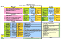
Mar. 4 (Sun)
Tutorial course includes fundamentals as well as current topics that would attract researchers in the each fields.
Assumed participants are not just the graduate students and beginners in the company, but also specialists in other fields and entrepreneurs of the start-ups.
| 12:30- |
Registration |
Tutorial Plasma Science 1,2
Chair:M. Aramaki
(Nagoya Univ., Japan)
<Room B> |
| 13:00-13:45 |
A. Kono (Nagoya Univ., Japan)
"Optical Diagnostics and Monitoring of Processing Plasmas" |
| 13:45-14:30 |
U. Czarnetzki (Ruhr-Univ. Bochum, Germany)
"Radio-Frequency Plasmas" |
| 14:30-14:40 |
Break |
Tutorial Nitride Semiconductors 1,2
Chair:H. Amano(Nagoya Univ., Japan)
<Room B> |
| 14:40-15:25 |
H. Amano (Nagoya Univ., Japan)
"Nitride-Based Visible LEDs" |
| 15:25-16:10 |
A. Khan (Univ. of South Carolina, USA)
"III-Nitride Technology, it’s requirements and commercialization" |
| 16:10-16:20 |
Break |
Tutorial Nanomaterials 1,2
Chair: M. Hiramatsu (Meijo Univ., Japan)
<Room B> |
| 16:20-17:05 |
J. G. Han (Sungkyunkwan Univ.,Korea)
"Fundamental and advanced plasma processes for thin film design and synthesis" |
| 17:05-17:50 |
M. Hiramatsu (Meijo Univ., Japan)
"Carbon Nanostructures: plasma synthesis and characterization" |
| 18:00-19:30 |
Welcome Party
(Student Cafeteria III, Chubu University) |
Mar. 5 (Mon)
| 9:00- |
Registration |
Opening
Chair:H. Masuda (Nagoya Inst. of Tech.,Japan)
<Room S> |
| 9:30-9:45 |
Opening
<Guest Address>
N. Kimura (Director for Regional R&D Promotion, Ministry of Education, Culture, Sports, Science and Technology, Japan)
<Organizer Address>
S. Kato (Tokai Region Knowledge Cluster Headquarters, Aichi Science & Technology Foundation, Japan)
<ISPlasma2012 Organizing Committee Chair Address>
M. Hori (Nagoya Univ., Japan) |
| 9:45-9:55 |
Opening Talk
Y. Ohtsuka (Tokai Region Knowledge Cluster Headquarters, Aichi Science & Technology Foundation, Japan) |
| 9:55-10:25 |
Knowledge Cluster Lecture
5a-S01C
Masaru Hori (Nagoya Univ., Japan) |
| 10:25-10:40 |
Break |
Plenary/Keynote Lecture
Chair:H. Amano (Nagoya Univ., Japan)
<Room S> |
| 10:40-11:20 |
Plenary Lecture
5a-S02PL
Atsuo Iiyoshi (Chubu Univ., Japan)
"How to Bring the Power of the Sun down to the Earth
~Fusion Plasma and Solar Energy Research~" |
| 11:20-11:55 |
Keynote Lecture
5a-S03K
Y. Nanishi (Ritsumeikan Univ., Japan/Seoul National Univ., Korea)
"Importance of Advanced Plasma for Frontier Nitride Semiconductor Technologies" |
| 11:55-12:30 |
Keynote Lecture
5a-S04K
P. Kamat (Univ. of Notre Dame, USA)
"Light Energy Conversion with Nanostructure Assemblies" |
| 12:30-13:15 |
Lunch |
| 13:15-14:45 |
Poster Session 1 |
| |
Plasma Science 1
Plasma Sources
and Diagnostics I
Chiar:K. Nakamura
(Chubu Univ., Japan)
<Room A> |
Nitride
Semiconductors 1
Growth of Nitrides
Chair:Y. Nanishi
(Ritsumeikan Univ., Japan/
Seoul National Univ., Korea)
<Room B> |
Nanomaterials 1
Nanocarbon
Materials
Chair:Y. Suda
(Toyohashi Univ. of
Tech., Japan)
<Room C> |
14:45-15:15
Invited Lecture
5p-A01IA
R. P. Brinkmann (Ruhr-Univ. Bochum, Germany)
"Active plasma resonance spectroscopy − electromagnetic vs. electrostatic concepts " |
14:45-15:15
Invited Lecture
5p-B01IB
T. Hashimoto (Sixpoint Materials, Inc., USA)
"Improved crystal quality of bulk GaN grown by the ammonothermal method" |
14:45-15:15
Invited Lecture
5p-C01IC
Y. Awano (Keio Univ., Japan)
"Remote Plasma CVD technologies for Carbon based LSI interconnects" |
15:15-15:35
5p-A02OA (2148)
Y. Liang (Chubu Univ., Japan)
"Curling probe monitoring of wall condition in plasma processing" |
15:15-15:35
5p-B02OB (2422)
N. Okada (Yamaguchi Univ., Japan)
"Optical properties of multiple quantum wells on GaN layers composed of {10-11} and m-facets structure" |
15:15-15:35
5p-C02OC (2416)
H. Tanoue (Toyohashi Univ. of Tech., Japan)
"Patterning of Tetrahedral Amorphous-Carbon Film by Electron Beam Lithography and Pick Up from Si-Wafer in Focused Ion Beam System" |
15:35-15:55
5p-A03OA (2166)
I. Ganachev ( Shibaura Mechatronics Corp.,Japan)
"Power dependence of electron dnesity profiles in surface-wave plasma studied by self-consistent numerical simulation with local plasma kinetics" |
15:35-15:55
5p-B03OB (2327)
S. Park (Seoul National Univ., Korea)
"Effects of high temperature GaN nucleation layers grown with different carrier gases on a-plane GaN by metal organic chemical vapor deposition" |
15:35-15:55
5p-C03OC (2159)
K. Yasuda (Nagoya Univ., Japan)
"Changes in crystalline structures of initial growth surfaces of carbon nanowalls" |
15:55-16:15
5p-A04OA (2206)
A. Fukushima (Nagoya Univ., Japan)
"Relationship between silicon thin film property and flux ratio of H radical to silicon growth precursor in SiH4/H2 plasma CVD" |
15:55-16:15
5p-B04OB (2223)
Y. Ryu (Kyushu Univ., Japan)
"Relationship between etch pits and threading dislocations in AlN grown on a sapphire substrate" |
15:55-16:15
5p-C04OC (2189)
G. Kalita (Chubu Univ., Japan)
"Synthesis of graphene by surface wave microwave plasma CVD for transparent electrode applications" |
| 16:15-16:35 |
Break |
| |
Plasma Science 2
Plasma Sources
and diagnostics II
Chair:R. P. Brinkmann
(Ruhr-Univ., Germany)
<Room A> |
Nitride Semiconductors 2
Optical Device and
Characterization
Chair:T. Hashimoto
(SixPoint Materials, Inc., USA)
<Room B> |
Nanomaterials 2
Porous Materials
Chair:M. Bratescu
(Nagoya Univ., Japan)
<Room C> |
| |
16:35-17:05
Invited Lecture
5p-A05IA
Vinu L. Venkatraman (EPFL, Switzerland)
"Chip-scale rubidium dielectric barrier discharge lamp for miniature atomic clocks and magnetometers" |
16:35-16:55
5p-B05OB (2034)
L. Lu (Nagoya Inst. of Tech., Japan)
"Significant variation of Electroluminescence emission with different barriers of AlxGa1-xN multiple-quantum-well in deep ultraviolet light-emitting diodes" |
16:35-17:05
Invited Lecture
5p-C05IC
S. Inagaki (Toyota Central R&D Labs., Inc., Japan)
"Nanoporous Organosilica Hybrids for Energy-related Applications" |
| |
17:05-17:25
5p-A06OA (2381)
F. Tochikubo (Tokyo Metropolitan Univ., Japan)
"Electrolysis with atmospheric pressure glow discharge as a plasma electrode" |
16:55-17:15
5p-B06OB (2405)
F. Tuomisto (Aalto Univ., Finland)
"In-grown point and extended defects in PA-MBE GaN and InN" |
17:05-17:25
5p-C06OC (2283)
T. Kanda (Nagoya Univ., Japan)
"Vertical Lamination of Carbon Nanowalls by Two-step Growth Method" |
| |
17:25-17:45
5p-A07OA (2215)
M. Blajan (Shizuoka Univ., Japan)
"Diagnostics of microplasma spatial and temporal distribution by emission spectroscopy" |
17:15-17:35
5p-B07OB (2433)
F. Fukuyo (Mie Univ., Japan)
"Growth of AlGaN MQWs as a Target for Deep-UV-Light Sources" |
17:25-17:45
5p-C07OC (2019)
E. Omurzak (Kumamoto Univ., Japan)
"Hollow carbon nano-onions by the pulsed plasma in liquid with tunable morphology and composition" |
Mar. 6 (Tue)
| 9:10- |
Registration |
| |
Plasma Science 3
Deposition and
Modification of Thin Film
Chair:M. Goeckner
(Univ. of Texas at Dallas, USA)
<Room A> |
Nitride Semiconductors 3
Electron Device I
Chair:K.Chen
(The Hong Kong Univ. of
Science and Tech., China)
<Room B> |
Nanomaterials 3
Energy Generation/
Storage Devices
Chair:N. Zettsu
(Nagoya Univ., Japan)
<Room C> |
9:30-10:00
Invited Lecture
6a-A01IA
A. Ito (National Inst. for Fusion Science, Japan)
"Formation and Classification of Amorphous Carbon by Molecular Dynamics Simulation" |
9:30-10:05
Keynote Lecture
6a-B01KB
T. Palacios (Massachusetts Inst. of Tech., USA)
"GaN Transistors: Transforming Electronics from THz to KV" |
9:30-10:00
Invited Lecture
6a-C01IC
H. Nishihara (Tohoku Univ., Japan)
"Nanocarbons for energy storage applications" |
10:00-10:20
6a-A02OA (2426)
S. Chen (Nagoya Univ., Japan)
"The role of hydrogen radical on plasma damaged gallium nitride" |
10:05-10:25
6a-B02OB (2302)
T. Kubo (Nagoya Inst. of Tech., Japan)
"Characterization of aluminum oxide deposited on GaN using ozone-based atomic layer deposition" |
10:00-10:20
6a-C02OC (2005)
A. Al-zubaidi (Nagoya Inst. of Tech., Japan)
"Ion Accessibility and the Resulting Electrical Double Layer Capacitance of Different Electrolytes Inside Open-end SWCNT" |
10:20-10:40
6a-A03OA (2242)
C. Lin (National Dong Hwa Univ., Taiwan)
"ZrO2 Resistive Switching Memory Fabricated on PES Flexible Substrate" |
10:25-10:45
6a-B03OB (2162)
U. Honda (Aichi Inst. of Tech. Japan)
"Comparision of deep levels in n-GaN grown by MOCVD on sapphire substrates with LT-AlN and GaN buffer layers |
10:20-10:40
6a-C03OC (2176)
H. Seo (Kyushu Univ., Japan)
"The improvement on the adhesion of Si nanoparticles
for Si quantum dot-sensitized solar cells" |
10:40-11:00
Break |
10:45-11:00
Break |
10:40-11:00
Break |
Plasma Science 4
Etching Process
Chair:A. Ito
(National Inst. for
Fusion Science, Japan)
<Room A> |
Nitride Semiconductors 4
Device Processing
Chair:Chair:M. Yamaguchi
(Nagoya Univ., Japan)
<Room B> |
Nanomaterials 4
Surface Modification/
Surface Functionalization
Chair:M. Shima
(Gifu Univ., Japan)
<Room C> |
11:00-11:30
Invited Lecture
6a-A04IA
R. Bruce (IBM T. J. Watson Research Center, USA)
"Plasma-Polymer Interactions For Nanoscale Patterning Of Materials" |
11:00-11:30
Invited Lecture
6a-B04IB
K. Chen (The Hong Kong Univ. of Science and Tech.,China)
"Fluorine Plasma Ion Implantation: a GaN Normally-off HEMT Technology" |
11:00-11:30
Invited Lecture
6a-C04IC
P. Mayrhofer (Montanuniversitaet Leoben, Austria)
"Computational Design and Experimental Study of Transition-Metal-Aluminum-Nitride Thin Films" |
11:30-12:00
Invited Lecture
6a-A05IA
M. Goeckner (Univ. of Texas at Dallas, USA)
"Plasma chemistry and film growth in a complex organic system" |
11:30-11:50
6a-B05OB (2163)
M. Niibe (Univ. of Hyogo, Japan)
"Damage Analysis of n-GaN Crystals Etched with He and N2 Plasma" |
11:30-11:50
6a-C05OC (2004)
H. Tamagawa (Gifu Univ., Japan)
"Bending controllability of Nafion-based IPMC coated with MnO2-coated CMC" |
12:00-12:20
6a-A06OA (2077)
E. Kunnen (imec, Belgium)
"Influence and evolution of 193i resist composition during VUV exposure" |
11:50-12:10
6a-B06OB (2044)
K. Hagiwara (Aichi Inst. of Tech., Japan)
"Carbon related local vibration mode in a (1-101)AlGaN grown on a (111)Si substrate" |
11:50-12:10
6a-C06OC (2230)
N. Zettsu (Nagoya Univ., Japan)
"PS@Au Plasmonic Nanoshells with Conical Shape for Highly-sensitive NIR-light responsible LSPR-sensor" |
| 12:10-13:00 |
Lunch |
| 13:00-14:30 |
Poster Session 2 |
Industry-Academia- Government Collaboration 1
Research Hub Establishment toward Sustainable Development
Chair:M. Takahashi (Chubu Univ., Japan)
<Room S>
*You can download the presentation data from the link below.
|
| 14:30-14:55 |
Keynote Lecture
6p-S01KE
T. Koljonen (VTT Technical Research Centre of Finland, Finland)
“Instruments for creating an innovation hot spot” |
| 14:55-15:20 |
Keynote Lecture
6p-S02KE
S. Ohmori (YRP International Alliance Inst., Japan)
”R&D Promotions at Yokosuka Research Park” |
| 15:20-15:45 |
Keynote Lecture
6p-S03KE
Y. Tai (Industrial Technology Research Institute, Taiwan)
"How does ITRI do for Formation of Industrial-Academia-Government Collaboration
A case of TAS (Taiwan Aerospace Supply chain Alliance) Formation" |
| 15:45-16:10 |
Keynote Lecture
6p-S04KE
T. Degawa (TECHNO INTEGRATION Co. Ltd, Japan)
"The trend of development and start‐up sites in the world and Japan
―The issues, competitiveness and prospect of innovatio in the context of MOT―" |
| 16:10-16:35 |
Keynote Lecture
6p-S05KE
W. Izumiya (Sangyo Times, Inc., Japan)
*The presentation data of Mr. Izumiya is not released through website.
"It should be driven forward to establish the domestic R&D Hubs
―Tokai Region as a Potential Location―" |
| 16:35-16:50 |
Break |
Industry-Academia-Government Collaboration2
Research Hub Establishment toward Sustainable Development
Chair:M. Takahashi (Chubu Univ.,Japan)
<Room S>
|
| 16:50-18:20 |
Panel Discussion
Establishment of Global Research Hub toward Sustainable Development
=MODERATOR=
N. Odake (Nagoya Inst. of Tech., Japan)
=PANELIST=
T. Degawa (TECHNO INTEGRATION Co. Ltd, Japan)
W. Izumiya (Sangyo Times, Inc., Japan)
T. Koljonen (VTT Technical Research Centre of Finland, Finland)
S. Ohmori (YRP International Alliance Inst., Japan)
Y. Tai (Industrial Technology Research Institute, Taiwan)
M. Hori (Nagoya Univ., Japan) |
| 18:30-20:00 |
Banquet (Student Cafeteria I, Chubu University) |
Mar. 7 (Wed)
| 9:10- |
Registration |
| |
Plasma Science 5
Emerging Plasma
Technology I
Chair:T. Kaneko
(Tohoku Univ.)
<Room A> |
Nitride Semiconductors 5
Nano structure
Chair:A. Wakahara
(Toyohashi Univ. of Tech,
Japan)
<Room B> |
Nanomaterials 5
Functional NanoMaterials
Chair:E. Miura-Fujiwara
(Univ. Hyogo, Japan)
<Room C> |
9:30-10:00
Invited Lecture
7a-A01IA
P. Favia (Univ. of Bari, Italy)
"Plasma processing of Materials for Life Sciences" |
9:30-10:00
Invited Lecture
7a-B01IB
K. Kishino (Sophia Univ., Japan)
"InGaN-based Nanocolumn Emitters" |
9:30-10:00
Invited Lecture
7a-C01IC
H. Yamaguchi Greenslet (Univ. of Florida, USA)
"New Magnetic Abrasives: Development and Precision Applications" |
10:00-10:20
7a-A02OA (2330)
M. Shiratani (Kyushu Univ., Japan)
"A-Si:H Schottky Cells with Quite Low Light Induced Degradation Fabricated by Multihollow Discharge Plasma CVD" |
10:00-10:20
7a-B02OB (2142)
J. Birch (Linkoping Univ., Sweden)
"Tailoring of AlInN Nanohelixes by Controlled Curvedlattice Epitaxial Growth" |
10:00-10:20
7a-C02OC (2300)
D. Wei (National Taipei Univ. of Tech., Taiwan)
"Solvent effect on the synthesized characters of FePt monodispersive nanoparticles" |
10:20-10:40
7a-A03OA (2398)
Y. Setsuhara (Osaka Univ., Japan)
"ICP-Assisted Sputtering with Inner-Type Low-Inductance Antenna for Low-Damage Reactive Deposion of Functional Films" |
10:20-10:40
7a-B03OB (2078)
P. Shields (Univ. of Bath, UK)
"Fabricaton and properties of etched GaN nanorods" |
10:20-10:40
7a-C03OC (2188)
M. Shima (Gifu Univ., Japan)
"CoPt Alloy Nanomagnets Crystalized on Carbon Microcoils" |
| 10:40-11:00 |
Break |
| |
Plasma Science 6
Emerging Plasma
Technology II
Chair:P. Favia
(Univ. of Bari, Italy)
<Room A> |
Nitride Semiconductors 6
Electron Device II
Chair:T. Hashizume
(Hokkaido Univ., Japan)
<Room B> |
Nanomaterials 6
Nanoparticles/Nano
wires/Nanorods
Chair:K. Makihara
(Nagoya Univ., Japan)
<Room C> |
11:00-11:30
Invited Lecture
7a-A04IA
T. Kaneko (Tohoku Univ., Japan)
"Biomedical applications of DNA-nanocarbon conjugates synthesized by gas-liquid interfacial plasmas" |
11:00-11:30
Invited Lecture
7a-B04IB
J. Suda (Kyoto Univ.,Japan)
"Group-III nitride/silicon carbide heterostructures -- MBE growth and device applications" |
11:00-11:30
Invited Lecture
7a-C04IC
X. Li (Peking Univ., China)
"Synthesis of nanostructured materials by hot and cold plasmas" |
11:30-11:50
7a-A05OA (2161)
H. Hashizume (Meijo Univ., Japan)
"Effect of atomic oxygen on inactivation of spores of P.digitatum by low-temperature atmospheric-pressure plasma" |
11:30-11:50
7a-B05OB (2219)
J. Jesudass (Nagoya Inst. of Tech., Japan)
"Investigation of trap states in in-situ MOCVD grown AlN/AlGaN/GaN MIS-HEMTs grown on Sapphire substrates" |
11:30-11:50
7a-C05OC (2140)
C. Hsiao (Linkoping Univ., Sweden)
"Core-Shell AlInN Nanorod Arrays Grown by Magnetron Sputter Epitaxy" |
11:50-12:10
7a-A06OA (2271)
O. Li (Nagoya Univ., Japan)
"By-Products Analysis for Degradation of Cellulose by Solution Plasma" |
11:50-12:10
7a-B06OB (2113)
K. Takeshita (Tokyo Metropolitan Univ., Japan)
"Charge-State Dependent Annealing of Plasma- Induced Defects in n-GaN" |
11:50-12:10
(11:50-12:10)
7a-C06OC (2208)
T. Suzuki (Nagoya Univ., Japan)
"Field Emission Properties of 10-nm Organic Nanopillars Fabricated by H2/N2 Mixture Gas Plasma Etching" |
| 12:10-13:00 |
Lunch |
| 13:00-14:30 |
Poster Session 3 |
Interdisciplinary 1
Advanced Nitride Devices
Chair:A.Khan (Univ. of South Carolina, USA)
<Room S>
|
| 14:30-15:05 |
Keynote Lecture
7p-S01KB
B. Daudin (CEA-Grenoble, France)
"GaN nanowires, GaN/AlGaN and InGaN/GaN nanowire heterostructures: growth, structural and optical properties" |
| 15:05-15:35 |
Invited Lecture
7p-S02IB
T. Hashizume (Hokkaido Univ., Japan)
"GaN-based MOS structures processed with plasma-assisted dry etching" |
| 15:35-16:05 |
Invited Lecture
7p-S03IB
Y. Saito, A. Yoshioka (Toshiba Corporation Semiconductor & Strage Products Company, Japan)
"GaN-HEMTs for Power Electronic Applications" |
| 16:05-16:25 |
7p-S04OB (2199)
Q. Wang (The Univ. of Tokushima, Japan)
"Influence of Dry Recess Process on Enhancement-mode GaN MOSFET" |
| 16:25-16:45 |
Break |
Interdisciplinary 2
Plasma Science and Nitride Semiconductors
Chair:M. Yamaguchi (Nagoya Univ., Japan)
<Room S> |
| 16:45-18:05 |
Panel Discussion
Application of Advanced Plasma Technology for Nitride Semiconductors III
-Importance and problem of plasma processing in nitride semiconductor devices-
=MODERATOR=
H. Amano (Nagoya Univ., Japan)
=PANELIST=
T. Hashizume (Hokkaido Univ., Japan)
T. Kachi (Toyota Central R&D Labs., Inc., Japan)
A. Khan (Univ. of South Carolina, USA)
L. Selvaraj (Nagoya Inst. of Tech.,Japan)
Y. Nanishi (Ritsumeikan Univ., Japan/Seoul National Univ., Korea)
Y. Saito (Toshiba Corp. Semiconductor & Strage Products Company, Japan)
J. Suda (Kyoto Univ.,Japan) |
Mar. 8 (Thu.)
| 9:10- |
Registration |
Interdisciplinary 3
Plasma assisted growth
Chair:B. Daudin (CEA-Grenoble, France)
<Room S> |
| 9:30-10:05 |
Keynote Lecture
8a-S01KD
J. Speck (Univ. of California Santa Barbara, USA)
"Progress in the MBE Growth of GaN − Materials and Devices" |
| 10:05-10:25 |
8a-S02OD (2432)
K. Wang (Ritsumeikan Univ., Japan)
"Free holes in Mg doped InN confirmed by thermopower experiments" |
| 10:25-10:45 |
8a-S03OD (2362)
T. Ohachi (Doshisha University)
“Self-ionization of nitrogen atoms from negatively baiased electrode for monitoreing nitrogen atom flux to use PA-MBE” |
| 10:45-11:00 |
Break |
Interdisciplinary 4
Advanced Carbon Materials
Chair: M. Hiramatsu (Meijo Univ., Japan)
<Room S> |
| 11:00-11:35 |
Keynote Lecture
8a-S04KD
M. Meyyappan (NASA Ames Research Center, USA)
"Plasma Nanotechnology: Past, Present, and the Future" |
| 11:35-12:05 |
Invited Lecture
8a-S05ID
M. Hasegawa (AIST, Japan)
"Low-temperature and large-area graphene synthesis by using microwave plasma CVD" |
| 12:05-12:25 |
8a-S06OD (2139)
T. Hagino (Nagoya Univ., Japan)
"Effect of electrode materials on Synthesis of nano-graphene by alcohol in-liquid plasma" |
| 12:25-13:30 |
Lunch |
Late News
Chair: M. Sekine (Nagoya Univ., Japan)
<Room S> |
| 13:30-14:00 |
8p-S01OLNA (3009)
C. Koshimizu (TOKYO ELECTRON YAMANASHI LTD, Japan)
"Measurement of heat fluxes to silicon wafer in plasma etching using low-coherence interferometry"
8p-S02OLNB (3024)
A. Jesudas (Nanyang Technological Univ., Singapore)
"Trapping Analysis by Pulsed Current-Voltage Characteristics for AlGaN/GaN HEMTs on 4-inch Si (111)"
8p-S03OLNC (3008)
J. Yang (Chang Gung Univ., Taiwan)
"Preparation and characterization of nano Pt-modified graphene fuel cell catalyst for methanol oxidation in alkaline solutions"
|
Green Innovation 1
Chair:Meyyappan(NASA Ames Research Center, USA)
<Room S>
 |
| 14:00-14:35 |
Keynote Lecture
8p-S01KD
R. Nemanich (Arizona State Univ., USA)
"Energy Conversion based on Thermionic and Photo-Electron Emission using Low Work Function Doped Diamond Films" |
| 14:35-15:05 |
Invited Lecture
8p-S02ID
A. Yoshikawa (Chiba Univ., Japan)
"Proposal of SMART III-Nitride Tandem Solar Cells with Using InN/GaN Magic Number Digital Alloys " |
| 15:05-15:35 |
Invited Lecture
8p-S03ID
V. Svrcek (AIST, Japan)
"Microplasma Induced Surface Engineering of Silicon Nanocrystals in Liquid Medium" |
| 15:35-16:05 |
Invited Lecture
8p-S04ID
T. Nozaki (Tokyo Inst. of Tech., Japan)
"Room Temperature Methane Conversion for Green Technology: Direct Synthesis of Methane to Methanol" |
| 16:05-16:25 |
Break |
Green Innovation 2
Chair:T. Inomata (Nagoya Inst. of Tech., Japan)
<Room S>
|
| 16:25-17:45 |
Panel Discussion
Advanced Plasma Nanotechnology towards Green Innovation
=MODERATOR=
T. Nozaki (Tokyo Inst. of Tech., Japan)
=PANELIST=
M. Kambara (The Univ. of Tokyo, Japan)
M. Meyyappan (NASA Ames Research Center, USA)
R. Nemanich (Arizona State Univ., USA)
V. Svrcek (AIST, Japan) |
| 17:45-18:05 |
Award |
| 18:05-18:15 |
Closing |
|