Plenary Speaker
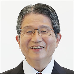 |
A. Fujishima (Tokyo University of Science, JAPAN) Water photolysis and photocatalysis |
Keynote / Invited Speakers
◆Keynote Speakers
 |
S. Hwang (Samsung, KOREA) Device applications of graphene and 2D materials |
 |
T. Kawai (Osaka University, JAPAN) Advanced nanodevices for single biomolecule detection--- Fabrication and Performance--- |
 |
K. Kishino (Sofia University, JAPAN) Progress of InGaN-based nanocolumns and visible nanoemitters prepared by rf-plasma assisted molecular beam epitaxy |
◆Tutorial SpeakersMar 6 Sun
 |
U. Czarnezki (Ruhr-Universitat Bochum, Institut fur Experimentalphysik V, GERMANY) Charged particle generation, transport, and fluxes in laboratory plasmas |
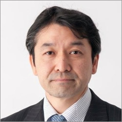 |
T. Ichiki (The University of Tokyo, JAPAN) Biosensing Devices: Microfluidic-based platform and beyond |
 |
K. Matsumoto (Taiyo Nippon Sanso Corp., JAPAN) Opportunities and Challenges to GaN MOCVD for Electron Devices |
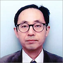 |
K. Shiraishi (Nagoya University, JAPAN) First Principles Theoretical Investigation of Future Nano-Materials |
 |
C. Wetzel (Rensselaer Polytechnic Institute, USA) The Challenge of the Green Gap – Development of Direct Emitting LEDs in the Green and Yellow Spectral Region |
◆Invited Speakers
S. Arulkumaran (Nanyang Technological University, SINGAPORE)
GaN Transistors on Silicon using Non-Gold process technology
T. Baba (Yokohama National University, JAPAN)
Nanolaser Biosensors
M. Bockowski (Unipress, POLAND)
HVPE-GaN Growth-Challenges and Perspectives
P. R. Cabarrocas (Ecole Polytechnique, FRANCE)
Vertical and in-plane silicon nanowires for radial junction solar cells and transistors produced in
a PECVD environment
P. Y. Chen (National Tsing Hua University, TAIWAN)
Synthesis of multi-functional surfaces inspired from carnivorous pitcher plants
Y. Darma (Institut Teknologi Bandung, INDONESIA)
Plasmon-exciton interaction and screening of exciton in ZnO-based thin film on different electronic environments
B. Daudin (CEA-Grenoble, FRANCE)
Carrier localization in nitride nanowire heterostructures
F. Faupel (Christian-Albrechts-Universität zu Kiel, GERMANY)
Plasma Deposition of Functional Nanocomposites
M. Germain (EpiGaN, BELGIUM)
GaN-on-Si technology for RF and Power Switching applications on large diameter substrates with SiN/AlGaN/GaN or SiN/AlN/GaN barriers grown by MOCVD
D. Go (University of Notre Dame, USA)
Plasmas with Liquid Electrodes: Fundamental Processes and Applications to Chemical Processing
S. Hara (Hokkaido University, JAPAN)
Axial Heterojunctions in Free-Standing Ferromagnetic MnAs/Semiconducting InAs Nanowires
T. Hashizume (Hokkaido University, JAPAN)
Interface control technologies for GaN power transistors
H. Hirayama (RIKEN, JAPAN)
Recent Progress and Future Prospects of AlGaN Deep-UV LEDs
Y. Honda (Nagoya University, JAPAN)
The growth of self-organized GaN nanowires on Si substrate by Molecular Beam epitaxy
S. Kaminaga (SPP Technologies Co., Ltd., JAPAN)
Plasma Processing Technology for MEMS and Trillion Sensors
M. Kasu (Saga University, JAPAN)
Diamond FETs for RF Power Electronics; Novel Hole Doping
Y. Kawakami (Kyoto University, JAPAN)
Assessment and control of recombination dynamics in nitride-based semiconductors for tailor-made solid state lighting
A. Koshio (Mie University, JAPAN)
Development of One-step Plasma Synthesis for Metal-free Carbon Nanotubes and Novel Nanocarbon Materials.
N. E. Lee (Sungkyunkwan University, KOREA)
Flexible and stretchable sensors for wearable electronics in personal healthcare
D. Li (Changchun Institute of Optics, CHINA)
Growth and Characterization of AlN on sapphire by high-temperature MOCVD
Z. Machala (Comenius University, SLOVAKIA)
Water activated by non-thermal air plasma discharges for bio-decontamination and bio-medical effects
A. Matsumoto (Tokyo Medical and Dental University, JAPAN)
”Borono-lectin” based approaches toward bio-sensing and drug delivery systems
A. Mizuno (Toyohashi University of Technology, JAPAN)
Electrostatics and non-thermal plasma for handling and processing of biological cells and molecules
M. Mozetič (Jožef Stefan Institute, SLOVENIA)
Selective functionalization of polymers with amino groups for excellent haemocompatibility of vascular grafts
D. Onoshima (Nagoya University, JAPAN)
Bioimaging devices for cell transplantation therapy in regenerative medicine
T. Osaki (KAST, JAPAN)
Microfluidics for Biosensing and healthcare applications
Y. Otoki (SCIOCS Company Ltd., JAPAN)
Improvement of electrical device performances by using epi-wafers grown on VAS-GaN substrate
S. W. Pang (City University of Hong Kong, HONG KONG)
Plasma Modified Electrodes on Neural Probes and Quasi 3D Plasmonic Biosensors
C. Pernot (Nikkiso, JAPAN)
Recent Progress of Nitrides DUV-LED
S. Rajan (The Ohio State University, USA)
Tunnel Junctions for Efficient Visible and UV Optoelectronics
O. Sakai (The University of Shiga Prefecture, JAPAN)
Plasma media created in abnormal-permeability metamaterial space
L. Schowalter (Crystal IS, Inc., USA)
Growth of Single-Crystal Aluminum Nitride as Substrates for Pseudomorphic UVC LEDs
C. Skierbiszewski (Unipress, POLAND)
Nitride based laser diodes grown by high nitrogen flux plasma assisted molecular beam epitaxy
K. Ueno (Saitama University, JAPAN)
Layered Chalcogenide Materials: Basic Properties and application to atomic-layer electronics
M. J. Wang (National Taiwan University of Science and Technology, TAIWAN)
Application of Nanoparticles on Biosensing
T. Wernicke (Technische Universität Berlin, GERMANY)
Deep UV Emitters
J. Xu (Nanjing University, CHINA)
Light Emission from Un-doped and Doped Nanocrystalline Si-based Multilayers
T. Yanagida (Kyushu University, JAPAN)
Single Crystalline Metal Oxide Nanowires and Their Promises
B. P. Zhang (Xiamen University, CHINA)
Loss study and fabrication of low-threshold GaN-based VCSELs
