
PROGRAM
*Program is subject to change.
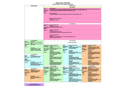
Please click the above to download the program.
1/28(Mon) | 1/29(Tue) | 1/30(Wed) | 1/31(Thu) | 2/1(Fri)
Poster Session 1 | Poster Session 2 | Poster Session 3 | Poster Session 4
Late News Poster Session 1 | Poster Session 2 | Poster Session 3 | Poster Session 4
Venue:Nagoya University (Higashiyama Campus)
Room A: Toyoda Auditorium
Room B: E & S Building
Room C: Noyori Conference Hall
Poster Session: Symposion (Toyoda Auditorium)
1/28(Mon)
| 12:30- | Registration |
| Tutorial Plasma Science Chair: H. Toyoda (Nagoya Univ., Japan) <Room C> |
|
| 13:00-13:45 | L. Overzet (The Univ. of Texas at Dallas, USA) "Fundamental aspects of high aspect ratio silicon etching" |
| 13:45-14:30 | K. Sasaki (Hokkaido Univ., Japan) "Introduction to advanced plasma diagnostics for material processing" |
| 14:30-14:40 | Break |
| Tutorial Nitride Semiconductors Chair: A. Wakahara (Toyohashi Univ. of Tech., Japan) <Room C> |
|
| 14:40-15:25 | J. Duboz (CRHEA-CNRS, France) "Light matter interaction in GaN" |
| 15:25-16:10 | Y. Nanishi (Ritsumeikan Univ., Japan / Seoul National Univ., Korea) "Recent developments in growth of InN and In-rich InGaN and future prospect" |
| 16:10-16:20 | Break |
| Tutorial Nanomaterials Chair: T.Shirafuji (Osaka City Univ., Japan) <Room C> |
|
| 16:20-17:05 | F. Fracassi (Univ. of Bari, Italy) "Nanomaterial preparation with nonequilibrium plasmas" |
| 17:05-17:50 | S. Iijima (Meijo Univ., Japan) "Nano carbon materials: science and applications" |
| 18:00-19:30 | Welcome Party 【Noyori Conference Hall, Nagoya University】 |
1/29(Tue)
| 9:00- | Registration | ||
| Opening Chair: H. Amano (Nagoya Univ., Japan) <Room A> |
|||
| 9:20-9:35 | Opening <Guest Address> T. Satomi (Director of University-Industry Cooperation and Regional R&D Division, Ministry of Education, Culture, Sports, Science and Technology, Japan) <Organizer Address> S. Kato (Tokai Region Knowledge Cluster Headquarters, Aichi Science & Technology Foundation, Japan) <ISPlasma2013 Organizing Committee Chair Address> M. Hori (Nagoya Univ., Japan) |
||
| 9:35-9:45 | Opening Talk Y. Ohtsuka (Tokai Region Knowledge Cluster Headquarters, Aichi Science & Technology Foundation, Japan) |
||
| 9:45-10:15 | Knowledge Cluster Lecture Tua-A01C M. Hori (Nagoya Univ., Japan) |
||
| 10:15-10:30 | Break | ||
| Plenary/Keynote Lecture Chair: S. Miyazaki (Nagoya Univ., Japan) <Room A> |
|||
| 10:30-11:10 | Plenary Lecture Tua-A02PL H. Ohno (Tohoku Univ., Japan) "Spintronics makes CMOS VLSI nonvolatile" |
||
| 11:10-11:40 | Keynote Lecture Tua-A03K J. G. Han (Sungkyunkwan Univ., Korea) "Challenge of plasma-nano technology for next generation frontier industry" |
||
| 11:40-12:10 | Keynote Lecture Tua-A04K R. Ruoff (The Univ. of Texas at Austin, USA), L. Colombo (Texas Instruments Inc., USA) "Graphene and h-BN at the Interface" |
||
| 12:10-13:20 | Lunch | ||
| 13:20-14:50 | Poster Session 1 | ||
| Plasma Science 1 Plasma Sources and Diagnostics I Chair: P. Chabert (LPP, CNRS Ecole Polytechnique, France) <Room A> |
Nitride Semiconductors 1 Crystal Growth of Nitrides I Chair: H. Amano (Nagoya Univ., Japan) <Room B> |
Nanomaterials 1 Nanocarbon and Nanomaterials Chair: M. Hiramatsu (Meijo Univ., Japan) <Room C> |
|
| 14:55-15:20 | Invited Lecture Tup-A01IA U. Czarnetzki (Ruhr Univ., Bochum, Germany) "Structured electrodes: Denser and more homogeneous plasmas" |
Invited Lecture Tup-B01IB R. Dwilinski (Ammono Company, Poland) "Bulk GaN substrates grown by ammonothermal method" |
Invited Lecture Tup-C01IC I. Lee (Chonbuk National Univ., Korea) "Localized surface plasmon mediated nanopillar light-emitting diode by Ag and Ag/SiO2 nanoparticles" |
| 15:20-15:40 | Tup-A02OA M. Shiratani (Kyushu Univ., Japan) "Time evolution of nanoparticle size in reactive plasmas: Comparison between theory and experiments" |
Tup-B02OB S. Kitagawa (Mie Univ., Japan) "Growth of thick AlN on 6H-SiC substrate by low-pressure HVPE" |
Tup-C02OC Y. Wang (National Cheng Kung Univ., Taiwan) "N-channel organic memory devices with TiO2 nanoparticles/polyimide insulator blends: Extra-high memory window" |
| 15:40-16:00 | Tup-A03OA R. W. Boswell (Space Plasma Power and Propulsion Laboratory, ANU, Australia) "Ideal low electron temperature plasma reactor" |
Tup-B03OB Y. Tomita (LayTec AG, Germany) "Strain engineering using in-situ curvature measurements and reduction of plastic deformation during the growth of GaN on various Si substrates" |
Tup-C03OC K. Nagashio (The Univ. of Tokyo, Japan) "Extraction of quantum capacitance in monolayer graphene" |
| 16:00-16:20 | Tup-A04OA Y. Yang (National Chiao Tung Univ., Taiwan) "A cold planar nitrogen atmospheric-Pressure plasma jet with enhanced UV emission and radical generation using short electrodes" |
Tup-B04OB I. Shin (Seoul National Univ., Korea) "Improved crytalline quality of low temperature GaN by using a pre-deposited indium layer" |
Tup-C04OC Y. Ding (Tokyo Inst. of Tech., Japan) "Silicon nanocrystal fabrication by using nonthermal plasma and application to hybrid Sinanocrystal/ P3HT solar cells" |
| 16:20-16:40 | Break | ||
| Plasma Science 2 Plasma Sources and Diagnostics II Chair: U. Czarnetzki (Ruhr Univ., Bochum, Germany) <Room A> |
Nitride Semiconductors 2 Crystal Growth of Nitrides II Chair: R. Dwilinski (Ammono Company, Poland) <Room B> |
Nanomaterials 2 Porous Materials and Hollow Nanofibers Chair: K. Makihara (Nagoya Univ., Japan) <Room C> |
|
| 16:40-17:05 | Invited Lecture Tup-A05IA P. Chabert (LPP, CNRS Ecole Polytechnique, France) "Modeling of atmospheric capacitive discharges in He/O2" |
Invited Lecture Tup-B05IB W. Walukiewicz (Lawrence Berkeley National Lab., USA) "In-rich group III-nitride alloys for solar power utilization devices" |
Invited Lecture Tup-C05IC T. Wei (Chung-Yuan Univ., Taiwan) "Rapid grafting of anti-biofouling and environment-responsive polymers by atmospheric-pressure plasmas" |
| 17:05-17:25 | Tup-A06OA N. Nishizawa (Nagoya Univ., Japan) "Ultrafast near-infrared spectroscopy using fiber laser based wavelength tunable narrowlinewidth source" |
Tup-B06OB Y. Kawai (Nagoya Univ., Japan) "Enhancement of growth rate in GaN homoepitaxy by plasma-assisted molecular beam epitaxy using high-density nitrogen radical source" |
Tup-C06OC F. Fracassi (Univ. of Bari, Italy) "Investigation of atmospheric pressure plasma-enhanced chemical vapor deposition from methyldisiloxane precursors" |
| 17:25-17:45 | Tup-A07OA A. Pandey (Chubu Univ., Japan) "Curling probe monitoring of plasma CVD and wall cleaning processes" |
Tup-B07OB T. Kumada (Tohoku Univ., Japan) "Influence of N2 gas flow ratio on crystalline quality of Al-polar AlN layer deposited using reactive magnetron sputtering" |
Tup-C07OC W. Diono (Nagoya Univ., Japan) "Direct formation of composite hollow nanomicrofibers from polymer by electrospinning" |
1/30(Wed)
| 9:10- | Registration | ||
| Plasma Science 3 Deposition and Modification of Thin Film Chair: H. Kondo (Nagoya Univ., Japan) <Room A> |
Nitride Semiconductors 3 Optical Devices Chair: E. Monroy (CEA-Grenoble, France) <Room B> |
Nanomaterials 3 Nanoparticles/ Nanowires/Nanorods Chair: T. Nozaki (Tokyo Inst. of Tech., Japan) <Room C> |
|
| 9:20-9:45 | Invited Lecture Wea-A01IA J. Duh (National Tsing Hua Univ., Taiwan) "From nanocomposite nitride to novel thin film metallic glass" |
Invited Lecture Wea-B01IB M. Pristovsek (Univ. of Cambridge, UK) "Low-cost high-efficiency GaN LEDs grown on 6- inch silicon" |
Invited Lecture Wea-C01IC C. Liu (Tianjin Univ, China) "Fabrication of metallic nano particles and nano composites via glow discharge plasma reduction: Current status and perspective" |
| 9:45-10:05 | Wea-A02OA W. Song (The Univ. of Tokyo, Japan) "Oxidation kinetics of Ge by oxygen radicals" |
Wea-B02OB T. Fujita (Panasonic Corporation, Japan) "Design of light-extracting texture and anisotropic dry etching of m-plane GaN LED" |
Wea-C02OC K. Koga (Kyushu Univ., Japan) "Single particle trapping in plasmas using laser for studying interaction between a fine particle and palsams" |
| 10:05-10:25 | Wea-A03OA H. Yamada (Diamond Research Lab. AIST, Japan) "Uniformity of the growth of single-crystal diamond wafers over inch size area by using reactive microwave plasma CVD" |
Wea-B03OB Withdrawn S. Kim (Korea Photonics Tech. Inst. (KOPTI), Korea) "High efficiency InGaN light-emitting diodes by using air void embedded SiO2 mask template" |
Wea-C03OC M. H. Mamat (Univ. Teknologi MARA, Malaysia) "Fabrication of high performance ZnO nanorod array-based UV photoconductive sensor by RF magnetron sputtering at different oxygen flow rates" |
| 10:25-10:45 | Break | ||
| Interdisciplinary 1 Advanced Carbon Materials Chair: Y. Suda (Toyohashi Univ. of Tech., Japan) <Room A> | |||
| 10:45-11:15 | Keynote Lecture Wea-A04KD Y. Lee (Sungkyunkwan Univ., Korea) "Observing graphene grain boundary by optical microscopy" |
||
| 11:15-11:40 | Invited Lecture Wea-A05ID S. Yamasaki (AIST, Japan) "Diamond film growth and electronic devices" |
||
| 11:40-12:00 | Wea-A06OD K. Higuchi (Nagoya Univ., Japan) "High-mobility carbon nanotube thin-film transistors fabricated on plastic film with flexographic printing technique" |
||
| 12:00-13:00 | Lunch | ||
| 13:00-14:30 | Poster Session 2 | ||
| Industry-Academia Government Collaboration 1 The Innovation Management Chair: M. Sekine (Nagoya Univ., Japan) <Room A>
|
|||
| 14:30-15:10 | Keynote Lecture Wep-A01KE S. Fujimura (Tokyo Inst. of Tech., Japan) "Management of technology for forming a global innovation base and developing human resources" |
||
| 15:10-15:40 | Keynote Lecture Wep-A02KE J. De Boeck (IMEC, Belgium) "Open innovation in nano-electronics through a global industrial partnership" |
||
| 15:40-16:10 | Keynote Lecture Wep-A03KE E. Yamaguchi (Doshisha Univ., Japan) "Three types of breakthrough innovations for creating future industries" |
||
| 16:10-16:40 | Keynote Lecture Wep-A04KE P. Feraboli (Automobili Lamborghini Laboratory at the Univ. of Washington, USA) "Conducting industrial R&D in academia: Challenges and opportunities" |
||
| 16:40-16:50 | Break | ||
| Industry-Academia Government Collaboration 2 Chair: S. Fujimura (Tokyo Inst. of Tech., Japan) <Room A>
|
|||
| 16:50-18:20 | Panel Discussion P. Feraboli (Automobili Lamborghini Laboratory at the Univ. of Washington, USA) |
||
| 19:00-20:30 | Banquet (South Cafeteria, Nagoya University) | ||
1/31(Thu)
| 9:10- | Registration | ||
| Plasma Science 4 Etching Process Chair: L. Overzet (The Univ. of Texas at Dallas, USA) <Room A> |
Nitride Semiconductors 4 Defect Analysis Chair: B. Daudin (CEA-Grenoble, France) <Room B> |
Nanomaterials 4 Surface Modification/Surface Functionalization Chair: M. Shima (Gifu Univ., Japan) <Room C> |
|
| 9:20-9:45 | Invited Lecture Tha-A01IA A. Eppler (Lam Research Corporation, USA) "Pulsed plasma applications in etch" |
Invited Lecture Tha-B01IB P. Ruterana (CIMAP UMR 6252 CNRS, ENSICAEN, CEA, France) "Mechanisms of damage formation during Rare Earth ion implantation in nitride semiconductors" |
Invited Lecture Tha-C01IC J. Cheng (IBM Almaden Research Center, USA) "Extending patterning capability using directed self-assembly" |
| 9:45-10:05 | Tha-A02OA S. Kumagai (Toyota Technological Inst., Japan) "3D wiring of vertically etched photo cell Islands for high voltage generation" |
Tha-B02OB A. Koizumi (Osaka Univ., Japan) "Luminescence properties of Eu-doped GaN grown by organometallic vapor phase epitaxy using a new Eu precursor bis(n- propyltetramethylcyclopentadienyl) europium" |
Tha-C02OC E. Yang (Shizuoka Univ., Japan) "Enhanced surface functionalization of graphite-encapsulated nanoparticles by RF plasma with Pulsed-biasing powder blowing method" |
| 10:05-10:25 | Tha-A03OA R. Kometani (Nagoya Univ., Japan) "High temperature plasma etching of GaN" |
Tha-B03OB H. Nykanen (Aalto Univ., Finland) "Degradation of optical properties of epitaxial GaN induced by vacancy activation under low energy electron beam irradiation" |
Tha-C03OC W. Kuo (National Taiwan Univ. of Science and Tech., Taiwan) "Surface modification using zwitterionic and PEG based copolymers to improve hemocompatibilty" |
| 10:25-10:45 | Break | ||
| Plasma Science 5 PlasmaBio and Medicine Chair: A. Mizuno (Toyohashi Univ. of Tech., Japan) <Room A> |
Nitride Semiconductors 5 Electron Devices Chair: Y. Nanishi (Ritsumeikan Univ., Japan / Seoul National Univ., Korea) <Room B> |
Nanomaterials 5 Functional NanoMaterials Chair: H. Sato (Nagoya Inst. of Tech., Japan) <Room C> |
|
| 10:45-11:10 | Invited Lecture Tha-A04IA A. Fridman (Drexel Univ., USA) "Plasma medicine: Fundamental physical and biochemical mechanisms of direct plasma interaction with living tissues." |
Invited Lecture Tha-B04IB T. Fujiwara (ROHM Co., Ltd., Japan) "Plasma-process on GaN-based field-effect transistors" |
Invited Lecture Tha-C04IC H. Kwon (EMPA, Switzerland) "Functionally graded dual-nanoparticulatereinforced metal matrix composites" |
| 11:10-11:30 | Tha-A05OA P. Favia (Inst. For Inorganic Methodologies & Plasmas (IMIP)-CNR, Italy) "Surface modification of 3D porous scaffolds for Tissue Engineering by means of different plasma processes" |
Tha-B05OB D. C. Peter Raj (Nagoya Inst. of Tech., Japan) "Fabrication of AlGaN/GaN HEMTs on 200 mm Si (111) substrate" |
Tha-C05OC B. Liaw (National Taiwan Univ. of Science and Tech., Taiwan) "Sythesis of high index facets nanoparticles for cholesterol sensing" |
| 11:30-11:50 | Tha-A06OA S. Maruyama (Nagoya Univ., Japan) "Potential of adipose tissue-derived stem cells and low temparature physical plasma for use in regenerative medicine" |
Tha-B06OB S. Ozaki (Fujitsu Laboratories Ltd., Japan) "Effect of ALD method on threshold voltage shift in AlGaN/GaN MIS-HEMTs" |
Tha-C06OC M. A. Bratescu (Nagoya Univ., Japan) "Graphene decorated with gold bimetallic nanoparticles in solution plasma" |
| 11:50-13:00 | Lunch | ||
| 13:00-14:30 | Poster Session 3 | ||
| Interdisciplinary 2 Advanced Nitride Semiconductors Chair: T. Kachi (Toyota CentralR&D Labs., Inc., Japan) <Room A>
|
|||
| 14:30-15:00 | Keynote Lecture Thp-A01KD N. Grandjean (EPFL, Switzerland) "Advanced nitride semiconductors" |
||
| 15:00-15:25 | Invited Lecture Thp-A02ID B. Daudin (CEA-Grenoble, France) "AlGaN and InGaN Nanowire heterostructures grown by plasma-assisted molecular beam epitaxy" |
||
| 15:25-15:50 | Invited Lecture Thp-A03ID H. Fujioka (Inst. of lndustrial Science, The Univ. of Tokyo, Japan) "Characteristics of GaN devices prepared by pulsed sputtering" |
||
| 15:50-16:15 | Invited Lecture Thp-A04ID T. Kikkawa (FUJITSU LABORATORIES LTD., Japan) "GaN HEMT for high frequency amplifier and power conversion" |
||
| 16:15-16:40 | Invited Lecture Thp-A05ID K. Chen (The Hong Kong Univ. of Science and Tech., China) "Device technology for GaN mixed-signal integrated circuits" |
||
| 16:40-17:00 | Break | ||
| Interdisciplinary 3 Perspective of Nitride Semiconductors ~The Role of Plasma Science and Nano Technology~ Chair: A. Wakejima (Nagoya Inst. of Tech., Japan) <Room A>
|
|||
| 17:00-18:15 | Panel Discussion
|
||
2/1 (Fri)
| 9:10- | Registration | ||
| Plasma Science 6 Emerging Plasma Technology Chair: N. Ohno (Nagoya Univ., Japan) <Room A> |
Nitride Semiconductors 6 Nano Structure Advanced Processing Chair: W. Walukiewicz (Lawrence Berkeley National Lab., USA) <Room B> |
Nanomaterials 6 Energy Generation / Storage Devices Chair: Y. Nishikitani (JX Nippon Oil & Energy Corporation, Japan) <Room C> |
|
| 9:20-9:45 | Invited Lecture Fra-A01IA M. C. M. van de Sanden (Dutch Inst. for Fundamental Energy Research, The Netherlands) "Power efficient plasma activation of CO2" |
Invited Lecture Fra-B01IB E. Monroy (CEA-Grenoble, France) "Single GaN-based nanowires for photodetection and sensing applications" |
Invited Lecture Fra-C01IC M. Nakayama (Nagoya Inst. of Tech., Japan) "Fabrication and electrochemical property of all solid-state Li polymer rechargeable battery" |
| 9:45-10:05 | Fra-A02OA E. Stamate (Technical Univ. of Denmark, Denmark) "Plasma assisted RF sputtering of lithium phosphorous oxynitride thin films for all-solidstate lithium ion batteries" |
Fra-B02OB W. Khalfaoui (Univ. François RABELAIS de Tours, France) "GaN surface protection during RTA annealing with GaON cap-layer" |
Fra-C02OC M. Seki (The Univ. of Tokyo, Japan) "Energy conversion between exciton and plasmon in ZnO quantum wells and Ag nanoparticles" |
| 10:05-10:25 | Fra-A03OA S. Cho (Tohoku Univ., Japan) "Control of plasma potential and fullerene clustering for high yield synthesis of nitrogen endohedral fullerene" |
Fra-B03OB Y. Hua (National Cheng Kung Univ., Taiwan) "GaN schottky barrier photodetectors with a lattice-matched Al0.82In0.18N intermediate layer" |
Fra-C03OC G. D. Temmerman (Dutch Inst. For Fundamental Energy Research, Netherlands) "Efficient nanostructuring of metals by low energy helium ions for advanced energy materials" |
| Late News Plasma Science Chair: N. Ohno (Nagoya Univ., Japan) <Room A> |
Late News Nitride Semiconductors Chair:T. Kubo (Nagoya Inst. of Tech., Japan) <Room B> |
Late News Nanomaterials Chair: M. Hiramatsu (Meijo Univ., Japan) <Room C> |
|
| 10:25-10:45 |
Fra-A04OLNA I. Suhariadi (Kyushu University) "Effects of nitrogen on crystal growth of sputter-deposited ZnO films for transparent conducting oxide" |
Fra-B04OLNB J. Birch (Linköping Univ.) "High quality GaN nanorods grown by liquidtarget reactive magnetron sputter epitaxy" |
Fra-C04OLNC N. Min (Korea Univ.) "Multi-walled carbon nanotube-mediated enhancement of photogenerated electron transport in a plasma-treated MWCNTs/TiO2 nanopowders hybrid electrode formed by onestep spray coating for dye-sensitized solar cells" |
| 10:50-12:20 | Poster Session 4 | ||
| 12:20-13:30 | Lunch | ||
| Energy Sesssion 1 Energy Revolution Chair: M. Hiramatsu (Meijo Univ., Japan) G. Kalita (Nagoya Inst. of Tech., Japan) <Room A>
|
|||
| 13:30-14:00 | Keynote Lecture Frp-A01KD T. Nozaki (Tokyo Inst. of Tech., Japan) "Plasma catalysis for next generation C1-Chemistry" |
||
| 14:00-14:25 | Invited Lecture Frp-A02ID Y. Nishikitani (JX Nippon Oil & Energy Corporation, Japan) "Recent developments and future prospects for organic solar cells" |
||
| 14:25-14:50 | Invited Lecture Frp-A03ID I. Mukhopadhyay (Pandit Deendayal Petroleum Univ., India) "Recent development in solar power in gujarat: Case study for large power plant and solar city" |
||
| 14:50-15:20 | Keynote Lecture Frp-A04KD L. Shaw (Illinois Inst. of Tech., USA) "Energy storage enabled by nanomaterials and advanced processing" |
||
| 15:20-15:30 | Break | ||
| Energy Sesssion 2 Energy Revolution Chair: T. Nozaki (Tokyo Inst. of Tech., Japan) <Room A>
|
|||
| 15:30-16:45 | Panel Discussion Towards Smart Enegy Cities 〈MODERATOR〉 T. Nozaki (Tokyo Inst. of Tech., Japan) 〈PANELIST〉 T. Matsumoto (Osaka Gas Co., Ltd., Japan) I. Mukhopadhyay (Pandit Deendayal Petroleum Univ., India) M. Nakayama (Nagoya Inst. of Tech., Japan) Y. Nishikitani (JX Nippon Oil & Energy Corporation, Japan) L. Shaw (Illinois Inst. of Tech., USA) W. Walukiewicz (Lawrence Berkeley National Lab., USA) |
||
| 16:45-16:55 | Award Presenter: M. Hori (ISPlasma2013 Organizing Committee Chairperson) Announcer: A. Wakahara(ISPlasma2013 Program Committee Chairperson) |
||
| 16:55-17:00 | Closing | ||