| |
 |
MEXT (Ministry of Education, Culture, Sports, Science and Technology)
Regional Innovation Cluster Program (Global Type)
〜 Tokai Region Nanotechnology Manufacturing Cluster 〜 |
 |
3rd International Symposium on Advanced
Plasma Science
and its Applications for Nitrides and Nanomaterials |
 |
|
|
March
6-9, 2011
Nagoya Institute of Technology, Nagoya, Japan
| Organizing Committee |
| Chairperson: |
Masaru
Hori, Plasma Nanotechnology Research Center, Nagoya University |
| Vice-Chairperson: |
Hideki Masuda,
Nagoya Institute of Technology
Hiroshi Amano, Nagoya University
Keiji Nakamura, Chubu University |
|
|
|


LINK FREE.
Please use this LINK banner.
|

|
Please click the above to download the program. |
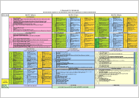
Mar. 6 (Sun)
| 17:30- |
Registration |
| 18:00-19:30 |
Welcome Party (Café Sala at Nagoya Institute of Technology) |
Mar. 7 (Mon)
| 8:45- |
Registration |
Opening/Plenary Lecture
Chair: H. Masuda (Nagoya Institute of Technology, Japan)
Room A |
| 9:15-9:30 |
Opening
<Guest Address>
Y. Tokiwa (Deputy Director-General, Ministry of Education, Culture,
Sports, Science and Technology, Japan)
<Organizer Address>
M.Matsuo (President, Aichi Science & Technology Foundation, Japan)
<ISPlasma2011 Organizing Committee Chair Address>
M. Hori (Nagoya University, Japan) |
| 9:30-9:40 |
Opening Talk
Y. Ohtsuka (Aichi Science & Technology Foundation, Japan)
"Tokai Region Nanotechnology Manufacturing Cluster and its Expansion Program" |
| 9:40-10:10 |
Plenary Lecture 7a-A01PL
Hiroyuki Sakaki (Toyota Technological Institute, Japan)
"From Superlattices to Quantum Dots: Roles of Nanostructures in Advanced Electronics and Photonics" |
| 10:10-10:30 |
Coffee Break |
Special Keynote Lecture/ Tokai Region Cluster Lecture
Chair: S. Noda (Aichi Science & Technology Foundation, Japan)
Room A |
| 10:30-11:00 |
Special Keynote Lecture 7a-A02SK
John Robertson (Cambridge University, UK)
"Applications of Carbon Nanotubes Grown by Chemical Vapor Deposition" |
| 11:00-11:20 |
Tokai Region Cluster Lecture 7a-A03C
M. Hori (Nagoya University, Japan)
"Fundamental Research and Global Innovation on Plasma Nanoprocessing" |
| 11:20-11:35 |
Tokai Region Cluster Lecture 7a-A04C
T. Egawa (Nagoya Institute of Technology, Japan)
"Study on AIGaN/GaN HEMT Grown on Si Substrate" |
| 11:35-11:50 |
Tokai Region Cluster Lecture 7a-A05C
O. Takai (Nagoya University, Japan)
"Material Development by Means of Solution Plasma" |
| 11:50-12:05 |
Tokai Region Cluster Lecture 7a-A06C
Y. Watanabe (Nagoya Institute of Technology, Japan)
"Drilling of Carbon Fiber Reinforced Plastic by Gyro-driven Metal-bonded Grinding Wheel" |
| 12:05-13:00 |
Lunch |
| 13:00-14:30 |
Poster Session 1 |
| |
Plasma Science and Technology 1
Advanced Plasma Measuring Technology
Chair: D. Graves (University of California, Berkeley, USA)
Room A |
Nitride Semiconductors 1
Plasma Assisted Growth
Chair: N. Grandjean (EPFL, Switzerland)
Room B |
Nanomaterials 1
Nanoparticles
Chair: T. Hihara (Nagoya Institute of Technology, Japan)
Room C |
14:30-15:00
Keynote Lecture
7p-A01KA
U. Czarnetzki (Ruhr-Univ, Bochum, Germany)
"Determination of Electron Densities by Diode Laser Absorption Spectroscopy" |
14:30-15:00
Keynote Lecture
7p-B01KB
B. Daudin (CEA Grenoble, France)
"Growth, Structural and Optical Properties of InGaN/GaN Nanowires" |
14:30-15:00
Keynote Lecture
7p-C01KC
M. Oda (ULVAC, Inc., Japan)
"Individually Dispersed Nanoparticles by Gas Evaporation and their Applications" |
15:00-15:30
Keynote Lecture
7p-A02KA
J. P. Booth (CNRS, France)
"Seeing Inside Plasma Etch Reactors: From Diagnostics to Sensors for Control" |
15:00-15:20
7p-B02OB
Y. Kawai (Nagoya University, Japan)
"Realization of Excellent Crystalline Quality of AlGaN Epilayer Grown on AlN Template by Plasma-Assisted Molecular Beam Epitaxy" |
15:00-15:20
7p-C02OC
R. Boswell (Australian National University, Australia)
"Low Temperature Sputtering of Nanocrystalline N-doped TiO2 Thin Films with Ar/O2/N2 Helicon Plasma" |
15:30-15:50
7p-A03OA
I. Liang (Chubu University, Japan)
"Electron Density Measurement by Novel Frequency Shift Probe" |
15:20-15:40
7p-B03OB
T. Ohachi (Doshisha University, Japan)
"Parallel Mesh Electrode to Monitor Nitrogen Atoms for Growth of III Nitride Semiconductors by PA-MBE" |
15:20-15:40
7p-C03OC
S. Yooyen (Mie University, Japan)
"Pulse Plasma CVD on the Growth of Nanorod" |
15:50-16:10
7p-A04OA
N. Sumi (Nagoya University, Japan)
"Real-time Electron-spin-resonance Measuremnt of Plasma Induced Surface Interactions" |
15:40-16:00
7p-B04OB
J. Birch (Linkoping University, Sweden)
"Ion-assisted Magnetron Sputter Epitaxy of Group III-nitrides" |
15:40-16:00
7p-C04OC
S. Machmudah (Kumamoto University, Japan)
"Gold and Silver Nanopaticles Produced by Pulsed Laser Ablation in Supercritical CO2" |
16:10-16:20
Coffee Break |
16:00-16:20
Coffee Break |
16:00-16:20
Coffee Break |
Plasma Science and Technology 2
Simulation
Chair: U. Czarnetzki (Ruhr-University Bochum, Germany)
Room A |
Nitride Semiconductors 2
Optical Devices
Chair: F. Ponce (Arizona State University, USA)
Room B |
Nanomaterials 2
Surface Modification/Surface Functionalization
Chair: K. Makihara (Nagoya University, Japan)
Room C |
16:20-16:50
Keynote Lecture
7p-A05KA
D. Graves (University of California, Berkeley, USA)
"Plasma-Surface Interactions at the Nanometer Scale" |
16:20-16:50
Keynote Lecture
7p-B05KB
N. Grandjean (EPFL, Switzerland)
"AlInN Alloy for Electronic and Optoelectronic Applications" |
16:20-16:50
Keynote Lecture
7p-C05KC
H. Takikawa (Toyohashi University of Technology, Japan)
"Super Hard Diamond-like Carbon Films; A State-of-the-Art" |
16:50-17:10
Keynote Lecture
S-Y. Kang
(Tokyo Electron Ltd. Technology Development Center)
"The Effect of Additional Database on Plasma Simulation for Etching Process" |
16:50-17:10
7p-B06OB
W. Y. Weng (National Cheng Kung University, Taiwan)
"High Responsivity GaN Nanowire-based UV Photodetectors" |
16:50-17:10
7p-C06OC
J-H. Jin (Korea University, Korea)
"Effects of Plasma Surface Functionalization on Biosensing Characteristics of A Fully-Integrated CNT-based Electrode System on Glass Substrate" |
17:10-17:30
Invited Lecture
7p-A07IA
Y. Tanaka (Kanazawa University, Japan) "Numerical Thermofluid Model of High-Power High-Pressure ICPs with Molecular Gases using Reaction Kinetics" |
17:10-17:30
7p-B07OB
H. S. Jeon (Korea Maritime University, Korea)
"UV LED with High Quality Epilayer grown by HVPE" |
17:10-17:30
7p-C07OC
C. Geffers (RWTH Aachen University, Germamy)
"Nanophase Hardfaced Coatings" |
| 17:30-19:00 |
Poster Session 2 |
Mar. 8 (Tue)
| 9:00- |
Registration |
| |
Plasma Science and Technology 3
Etching Process I
Chair: F. Laermer (Robert Bosch GmbH, Germany)
Room A |
Nitride Semiconductors 3
Device Characterizations
Chair: Y. Tokuda (Aichi Institute of Technology, Japan)
Room B |
Nanomaterials 3
Litium-ion Rechargeable Battery Cells
Chair: S. Kawasaki (Nagoya Institute of Technology, Japan)
Room C |
9:20-9:50
Keynote Lecture
8a-A01KA
M. J. Goeckner (University of Texas, Dallas, USA)
"An Improved Understanding of Fluorocarbon Plasmas" |
9:20-9:50
Keynote Lecture
8a-B01KB
F. Ponce (Arizona State University, USA) "Polarization Effects in Group-III Nitride Semiconductor Heterostructure Devices" |
9:20-9:50
Keynote Lecture
8a-C01KC
A. Yoshino (Asahi Kasei Corporation, Japan)
"Latest trends of Lithium Ion Battery Technology and Market" |
9:50-10:20
Keynote Lecture
8a-A02KA
A. Wendt (University of Wisconsin - Madison, USA)
"Control of Bombarding Ion Energy Distributions in Plasma Processing" |
9:50-10:10
8a-B02OB
Z. Chen (Nagoya Institute of Technology, Japan)
"Optical Properties and Deep Traps of InAlN Lattice-Matched to GaN Grown by MOCVD" |
9:50-10:10
8a-C02OC
N. Imanishi (Mie University, Japan)
"High Performance Si/Disordered Carbon with CNFs Composites for Lithium Ion Batteries" |
10:20-10:40
8a-A03OA
K. Hirota (Hitachi, Ltd., Japan)
"Study of Process Drift Caused by Ti Residue on Reactor Walls in Metal Gate Ethcing" |
10:10-10:30
8a-B03OB
Y. Nakano (Chubu University, Japan)
"Correlation between Current Collapses and Deep-Level Defects in AlGaN/GaN Hetero-Structures Probed by Photo-Capacitance Spectroscopy" |
10:10-10:30
8a-C03OC
Z. Quan (Nagoya Institute of Technology, Japan)
"Electrochemical property of LiCoO2 thin films composed of nanoparticles" |
10:40-10:50
Coffee Break |
10:30-10:50
Coffee Break |
10:30-10:50
Coffee Break |
Plasma Science and Technology 4
Etching Process II
Chair: M. J. Goeckner (University of Texas, Dallas, USA)
Room A |
Nitride Semiconductors 4
GaN/Si and its Applications
Chair: K. Inoue (Panasonic Corporation, Japan)
Room B |
Nanomaterials 4
Porous Materials
Chair: T. Inomata (Nagoya Institute of Technology, Japan)
Room C |
10:50-11:20
Keynote Lecture
8a-A04KA
F. Laermer (Robert Bosch GmbH, Germany)
"BOSCH-DRIE: Impact on MEMS and Applications" |
10:50-11:20
Keynote Lecture
8a-B04KB
A. Krost (Otto von Guericke University Magdeburg, Germany)
"Present and Future of GaN-on-Si" |
10:50-11:20
Keynote Lecture
8a-C04KC
H-C. Zhou (Texas A&M University, USA) "Metal-Organic Frameworks for Gas Storage and Separation" |
11:20-11:40
8a-A05OA
J. Ladroue (GREMI-STMicroelectronics, France)
"Deep Gallium Nitride Etching: Ways to Avoid Etching Defects" |
11:20-11:40
Invited Lecture
8a-B05IB
S. Arulkumaran (Nanyang Technological University, Singapore)
"High Off-state Breakdown Characteristics of AlGaN/GaN HEMTs on 4-inch Si" |
11:20-11:40
Invited Lecture
8a-C05IC 10418
S. Furukawa (Kyoto University, Japan)
"An Entangled Porous Framework As a Luminescent Sensor" |
11:40-12:00
8a-A06OA
X. Li (University of Glasgow, Schotland)
"A Low Damage Etchig Process of Sub-100 nm Platinum Gate Line for III-V MOSFET Fabrication and the Optical Emission Spectrometry of the Inductively Coupled Plasma of SF6/C4F8" |
11:40-12:00
8a-B06OB
Y. Liu (Sun Yat-sen University, China)
"Normally-off AlGaN/GaN HFETs on Si (111) Substrate Fabricated by Selective Area Growth Technique" |
11:40-12:00
Invited Lecture
A. Takeno (Gifu University, Japan)
"Nano Porous Plymer Film and Fiber by Craze Processing" |
| 12:00-13:00 |
Lunch |
| 13:00-14:30 |
Poster Session 3 |
Nitride Semiconductors 5
Recent Progress in Nitride Devices
Chair: M. Higashiwaki (National Institute of Information and Communications Technology, Japan)
Room A |
| 14:30-15:00 |
Keynote Lecture
8p-A01KB
A. Khan (Unversity of South Carolina, USA)
"Recent Progress of Nitride Semiconductor Devices and the Role of Plasma Science and Technology" |
| 15:00-15:30 |
Keynote Lecture
8p-A02KB
D. Alquier (Université de Tours, France)
"Recent Progresses in GaN Power Rectifier" |
| 15:30-16:00 |
Keynote Lecture
8p-A03KB
D. Ueda (Panasonic Corporation, Japan)
"Renovating Power Electronics by III-Nitride Devices" |
| 16:00-16:30 |
Keynote Lecture
8p-A04KB
H. Amano (Nagoya Unversity, Japan)
"Plasma Assisted Molecular Beam Epitaxial Growth of Thick InGaN Films and InGaN Nanorods for Future Light Source" |
| 16:30-16:50 |
Coffee Break |
Nitride Semiconductors 6
Plasma Science and Nitride Semiconductors II
Chair: M. Iwasaki (Nagoya Institute of Technology, Japan)
Room A |
| 16:50-18:10 |
Panel Discussion
Application of Advanced Plasma Technology for Nitride Semiconductors II
Succeeding to ISPlasma2010, the role of plasma science and technology for applications to nitride semiconductors such as; plasma processing for device fabrication and nitrogen radical source for crystal growth and others will be discussed.
<Moderator>
Y. Nanishi (Ritsumeikan Unversity, Japan/Seoul National Unversity, Korea)
<Panelists>
D. Alquier (Université de Tours, France)
H. Amano (Nagoya Unversity, Japan)
B. Daudin (CEA Grenoble, France)
N. Grandjean (EPFL, Switzerland)
H. Kano (NU Eco Engineering Co., Ltd., Japan)
A. Khan (Unversity of South Carolina, USA)
E. Monroy (CEA Genoble, France)
Y. Tokuda (Aichi Institute of Technology, Japan)
D. Ueda (Panasonic Corporation, Japan)
A. Uedono (Tsukuba Unversity, Japan)
|
| 18:30-20:00 |
Banquet (SAPPORO NAGOYA BREWERY KOUYOUEN) |
Mar. 9 (Wed)
| 9:00- |
Registration |
| |
Plasma Science and Technology 5
Thin Film Deposition Process
Chair: M. Kondo (AIST, Japan)
Room A |
Nitride Semiconductors 7
III-Nitride Microstrucrures
Chair: A. Subramaniam (Nanyang Technological University, Singapore)
Room B |
Nanomaterials 5
Composite/Functionally Grade Materials
Chair: E. Miura (Nagoya Institute of Technology, Japan)
Room C |
9:20-9:50
Keynote Lecture
9a-A01KA
J. G. Han (Sungkyunkwan Unversity, Korea)
"Novel Plasma Processes for Functional Thin Films for Flexible Electronics" |
9:20-9:50
Keynote Lecture
9a-B01KB
F. Scholz (Ulm University, Germany)
"Semipolar GaInN Quantum Well Structures on Large Area Substrates" |
9:20-9:50
Keynote Lecture
9a-C01KC
K. Mizuuchi (Osaka Municipal Technical Research Institute, Japan)
"Densification and Development of Synthesis Route for Enhancing Performance of Heat Dissipative Metal Matrix Composites in Continuous Solid-Liquid Co-Existent State" |
9:50-10:20
Keynote Lecture
9a-A02KA
J. Vlcek(Unversity of West Bohemia, Czech Republic)
"Pulsed Magnetron Deposition of High-Temperature Si-B-C-N Films" |
9:50-10:10
9a-B02OB
C. Lin (National Chung Hsing University, Taiwan)
"Micro-Square-Array InGaN-based Light-Emitting Diode with an insulated Ga2O3 Layer Through a Photoelectrochemical Process" |
9:50-10:10
9a-C02OC
H. Sato (Nagoya Institute of Technology, Japan)
"Effects of Dispersoids on Wear Behavior of Cu-based Composite Containing SiO2 Particles" |
10:20-10:40
9a-A03OA
Kusumandari (Nagoya Unversity, Japan) "Characterization of Damages of Al2O3/Ge Gate Stacks Structure Induced with Light Radiation during Plasma Nitridation" |
10:10-10:30
9a-B03OB
T. Araki (Ritsumeikan Unversity, Japan)
"TEM Study on Microstructure of Mg-doped InN Grown by RF-MBE Using DERI Method" |
10:10-10:30
Invited Lecture
Y. Ishikawa (JFCC)
"White Photoluminescence from Carbon Incorporated Silica" |
10:40-11:00
9a-A04OA
Y. H. Kwon (Sungkyunkwan University, Korea)
"Electrical properties of the nickel oxide correlated with point defects
induces by growth temperature and gas atmosphere" |
10:30-10:50
Coffee Break |
10:30-10:50
Coffee Break |
Nitride Semiconductors 8
Growth of GaN and Related Materials
Chair: F. Scholtz ((Ulm University, Germany)
Room B |
Nanomaterials 6
Nanocarbon Materials
Chair: H. Takikawa (Toyohashi University of Technology, Japan)
Room C |
11:00-11:10
Coffee Break |
Plasma Science and Technology 6
Solar Cells Based on Plasma Science
Chair: J. G. Han (Sungkyunkwan University, Korea)
Room A |
10:50-11:20
Keynote Lecture
9a-B04KB
E. Yoon (Seoul National Unversity, Korea) "Growth of Less Bowed GaN Using InN Interlayer by MOCVD" |
10:50-11:20
Keynote Lecture
9a-C04KC
S. Iijima* (Meijo Univ., Japan)
"Nanocarbon Materials: Synthesis, Characterization and Application"
*The following lecture has been canceled. M. Meyyappan (NASA Ames
Research Center, USA)""Plasma Nanotechnology: Past, Present, and the
Future" |
11:10-11:40
Keynote Lecture
9a-A05KA
M. Kondo (AIST, Japan)
"Plasma Processing for Innovative PV Technologies" |
11:20-11:40
9a-B05OB
Y. Tomita (LayTec GmbH, Germany)
"In-situ Measurement of Wafer Bow and GaN Surface Temperature -how MOCVD Process Parameters Influence the Uniformity of LED Wafers" |
11:20-11:40
9a-C05OC
H. Kondo (Nagoya Unversity, Japan)
"Study on Crystallographic Features of Carbon Nanowalls using Synchrotron X-ray" |
11:40-12:00
9a-A06OA
M. Sato (Kyushu Unversity, Japan)
"Generation of Nitridated Silicon Nano-Particles by Double Multi-Hollow Discharge CVD" |
11:40-12:00
9a-B06OB
T. Kawamura (Mie Unversity, Japan)
"Molecular Dynamics Simulation of Solution Growth of GaN" |
11:40-12:00
9a-C06OC
T. Kato (Tohoku Unversity, Japan)
"Novel Approch for Detailed Structure Control of Single-Walled Carbon Nanotubes based on Time-Programmed Plasma CVD" |
| 12:00-13:00 |
Lunch |
| 13:00-14:30 |
Poster Session 4 |
Industry-Academia-Government Collaboration 1
Global Open Innovation 1
Chair: E. Hamada (Nagoya Institute of Technology, Japan)
Room A
*You can download the presentation data from the link below. |
| 14:30-15:00 |
Keynote Lecture
T. Arimoto (JST, Japan)
"Japan's New Science and Innovation Policy under the Changing World -Beyond the Boundaries for Innovation- " |
| 15:00-15:05 |
Keynote Lecture
C. Mantel (Selantek, Inc., USA) *Lecture by Dr. Mantel has been canceled.
Explanation by K. Yoshimiura (ASTF)
"Semiconductor Manufacturing -Future Technology-" |
| 15:05-15:35 |
Keynote Lecture
W. Vandervorst (IMEC, Belgium)
"Imec, a Research Center with Flexible Business Opportunities Balancing between Fundamental Research, Advanced Technology and Innovative Applications" |
| 15:35-16:05 |
Keynote Lecture
W. Izumiya (Sangyo Times Inc., Japan)
*The presentation data of Mr. Izumiya is not released through website.
"Current Situation and Direction for Development on Semiconductor Industry in Asia/Japan" |
| 16:05-16:30 |
Keynote Lecture
M. Hori (Nagoya University, Japan)
"Foundation of Global Innovation Research Center for Advanced Plasma Science and Technology" |
| 16:30-16:40 |
Coffee Break |
Industry-Academia-Government Collaboration 2
Global Open Innovation 2
Chair: H. Toyoda (Nagoya University, Japan)
Room A
*You can download the presentation data from the link below.
|
| 16:40-18:00 |
Panel Discussion
Establishment of Advanced Plasma Science and Technology Center toward Open Innovation
After reports by specialists from various fields related to open innovation, the way towards establishing an advanced plasma nanotechnology science research foundation in the Tokai region through open innovation will be discussed.
<Moderator>
N. Odake (Nagoya Institute of Technology, Japan)
<Panelists>
T. Arimoto (JST, Japan)
M. Hori (Nagoya University, Japan)
W. Izumiya (Sangyo Times Inc., Japan)
Y. Madokoro (Aichi Prefectural Government, Japan)
C. Mantel (Selantek, USA)
W. Vandervorst (IMEC, Belgium) |
| 18:00 |
Closing |
|
|
|
Secretariat:c/o Aichi Science & Technology Foundation
Phone:+81-52-231-1656 Fax:+81-52-231-1640 E-mail:isplasma@astf.or.jp |
|
|
|